Google Pixel Buds teardown and thoughts on humanizing computer interaction
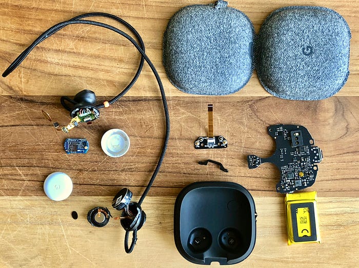
Google recently launched their wireless earbuds as a bold new step to enable Google’s “virtual personal assistant” through a wearable product.

I’ve talked previously about the promise of voice interfaces, and I believe in creating a more seamless human-computer interface to humanize technology, so I applaud this effort.

But to deliver the best AI-focused services even a software giant would need to break into the real world with a device one would feel comfortable wearing. But putting technology on one’s body is tough to get right — so it’s interesting to see how two leading technology companies approach this.


Generally wearables that try imbue the essence of something we’d actually wear end up facing a choice of looking like either jewelry or clothing. The Apple AirPods have been commented on as feeling like earrings (with the hanging microphone, their shiny metal accent, and needing to be delicately removed and placed into their case after use), and hence may fall into the jewelry category. If so, the Pixel Buds have taken a decidedly more “clothing” approach, with a soft fabric case, round button-like earpieces, and a string with a thoughtfully placed bead, which can be pulled on either end to snugly adjust the fit like a drawstring.
Meeting both the design and voice assistant requirements would require some thoughtful hardware engineering to get right, so naturally I got hold of a pair to teardown over the holiday, and to see how Google scored on these fronts…
Unboxing
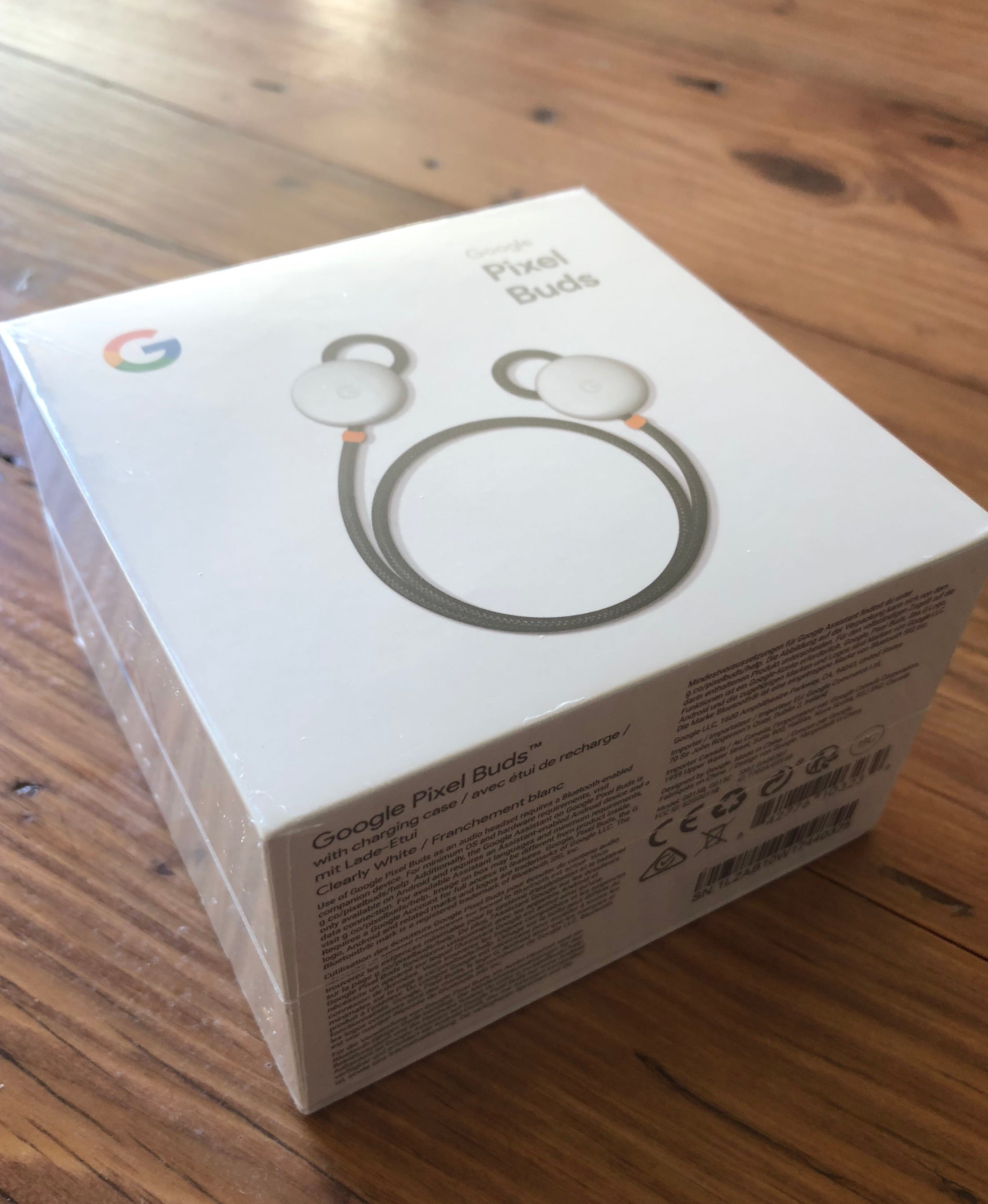
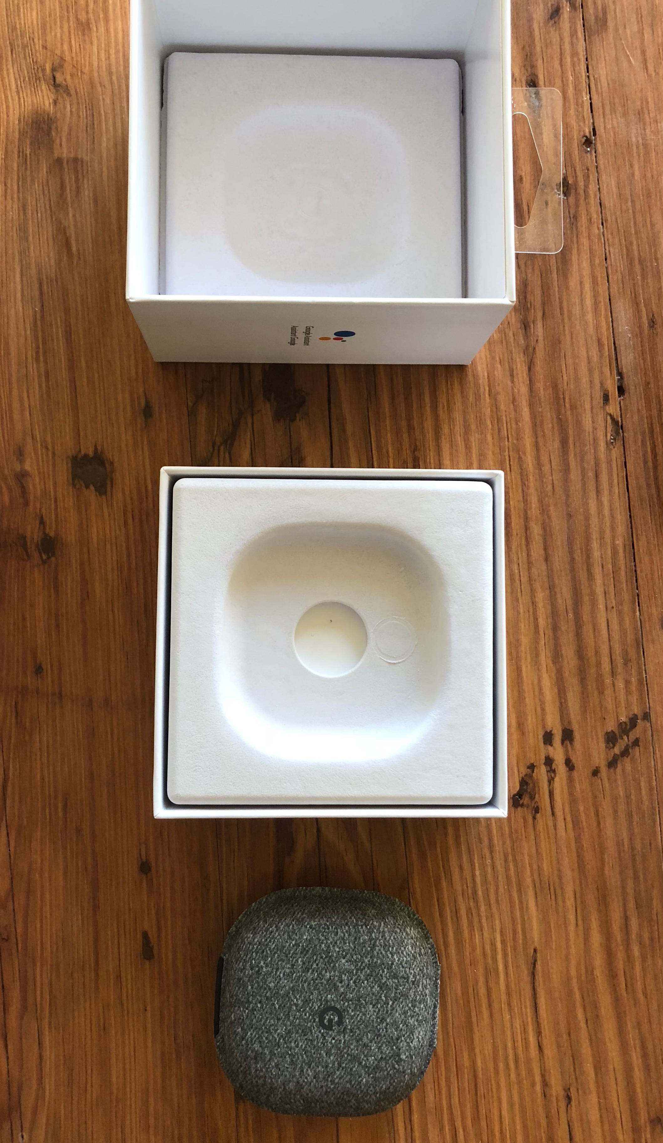
Nothing too outlandish with the packaging to write about here, just some pulp trays neatly nesting a fabric clamshell case, holding the earbuds.
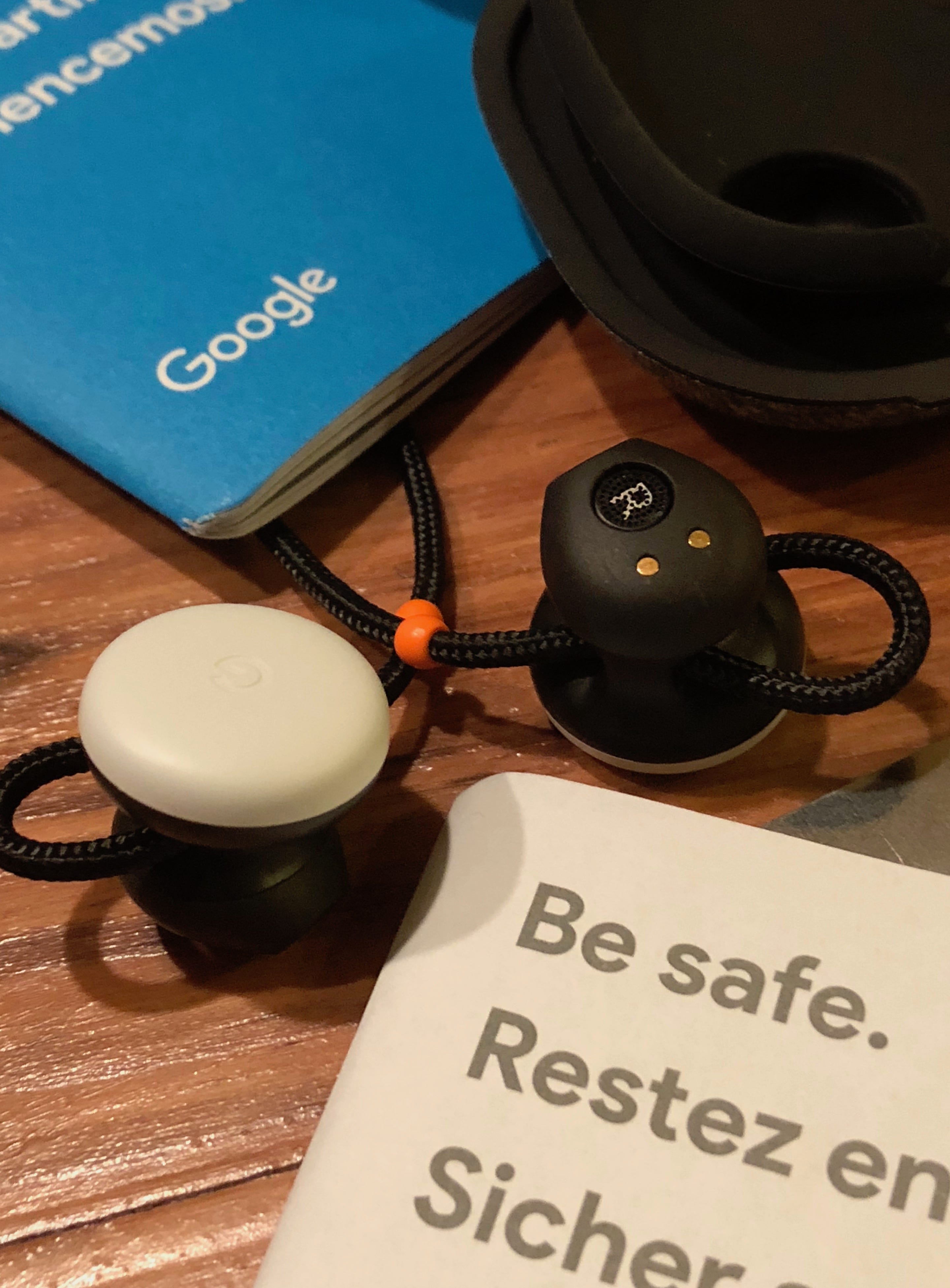
The earbuds are meant to rest outside the ear canal, and so there is no need for a tray of interchangeable silicone tips which one always ends up losing. But to go this route relies on the earbuds fitting and staying in your ear. The adjustable string loop was surprisingly effective at this, and kept the earbuds in securely during a run, with the orange bead cleverly acted as a limit to how far the cord could be pulled. Overall the cord seemed like a really neat design feature, adding to the soft material feel of the product, but had two suprising drawbacks:
- It looked so much like regular string, some users reportedly tried to cut the string and so Google had to explicitly warn people not to, and probably why they refer to it as a “cord” and not a string. In the teardown below you’ll see why cutting this is a bad idea…
- They don’t quite hang around your neck. The Pixel Buds are too end-heavy, with the supple string not giving much resistance, resulting in them frequently slipping off your neck on either side. The Beats X got this right, with a semi-rigid loop to fit around your neck, and in-ears that securely clip together magnetically when hanging around your neck. Product idea: an after-market leather/fabric collar that can go across the back of your neck and the cord can clip through to prevent them sliding off…
While most are not comfortable with PDA (public digital assistant, hat-tip to @karaswisher for the term), you can hear yourself and your surroundings well while wearing these, making it feel much more natural to talk while wearing. But not having a Pixel phone, there was not much testing of the assistant I could do beyond controlling music and Siri.
Being eager to take a look inside, I wasn’t going to wait till I could test these with a Pixel phone. So, onto the teardown…
The Teardown
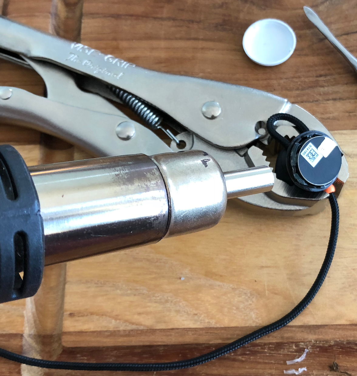
One could assume the earbuds were held together with some sturdy glue or adhesive, which would reliably seal the product and provide some level of waterproofing, so to open up would require highly localized heat. My weapon of choice? A hot air rework station. This is essentially similiar to a small hairdryer (but should never be used as one!) and is primarily for applying controlled heat onto specific areas of PCB’s, allowing one to remove or replace electronic components by melting the metal solder attaching them. They typically come with fairly accurate temperature control, so you can scale this way down to find a temperature that won’t melt the plastic, yet will soften any stubborn adhesive.
I decided to start with the left earbud, predicting that without microphones or a touch interface, this would be the lower tech side and so would have less to damage with my first attempt…
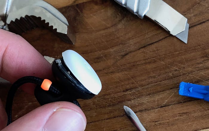
Prying open the cover, one can see what looks like the battery. Being glued in itself, this will need some more carefully applied heat and surgery to pry away from the plastic to see what lies beneath.

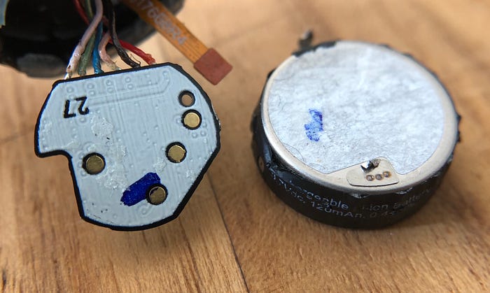
Pulling away what we can now identify as a 120mAh Li-ion battery, and unplugging the flex cable gives us a better view of the PCB with some basic components, and some wiring.

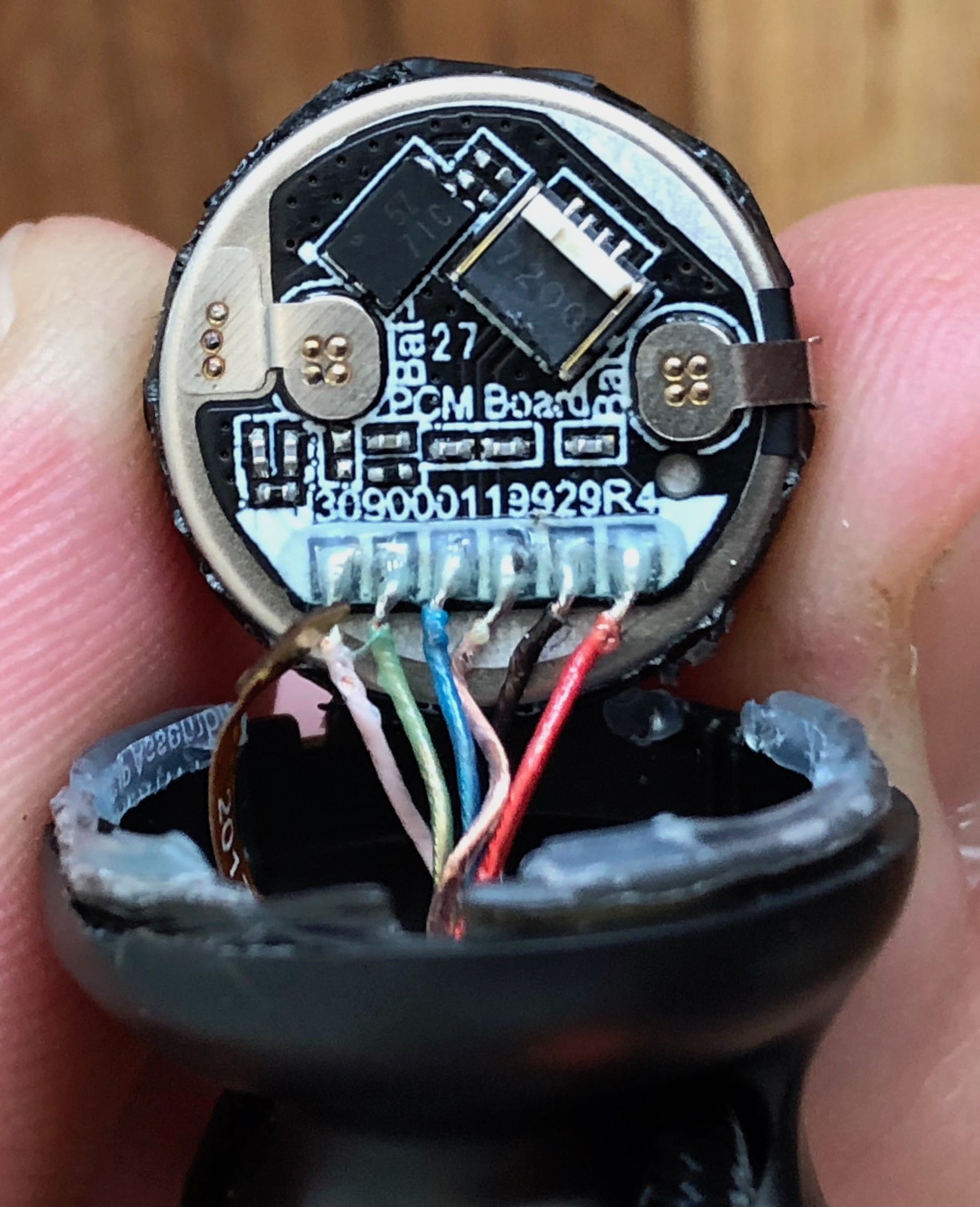
From this view we can assume that this left bud is in fact just the battery, leaving little space for any other advanced electronics. The 6 colored wires likely connect through the string to the other bud, and so would carry power and speaker signals. These wires are braided, i.e. made up of many strands twisted together, which provides suppleness allowing the string to be easily and repeatedly bent without damage.
Why are these just seemingly manually soldered directly to the PCB — surely Google would be more professional and use a header? There are a few reasons for this. Audio connections require good contact to limit noise — a blob of molten metal provides a much better contact than metal just pressing against another metal surface. There is also the risk of disconnecting or loosening after assembly — and if you have a good test procedure, you’d want to reliably attach the wires and never look back, yielding a removable header pointless. A header adds cost and takes up space. Also, soldering directly to the board enables you to easily cover the connections with a conformal coating or encapsulation, as seen, which provides some extra strength, insulation and humidity protection.
The flex cable however, is essentially a PCB of copper tracks on a flexible substrate. This is much cheaper for short distances where there isn’t going to be repetitive motion or twisting, and unlike wires, can be reliably attached to a PCB on either end by slipping into a low-cost and low-profile header.
Detaching the PCB from the battery reveals the silk-screened reverse and some test points. SIlkscreen, usually used for printing designators, may have been used to offset the test points from the surface, preventing accidental contact. Nothing much to see here.
Continuing the teardown, you can see the cables appear to be sealed in some type of encapsulant. This provides some strain relief, so that pulling on the cord will not result in any force pulling the wires off their connection to the PCB, and no doubt waterproofing.
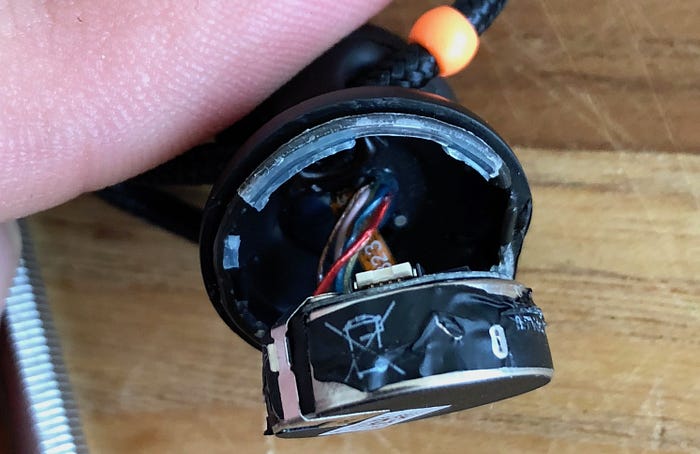
I tried to apply some heat to this to attempt to dig through, but the plastic appeared to start softening before the encapsulating material, meaning it must be some form of epoxy and not glue. We’ll have to take a look at where these cables go from the other side.
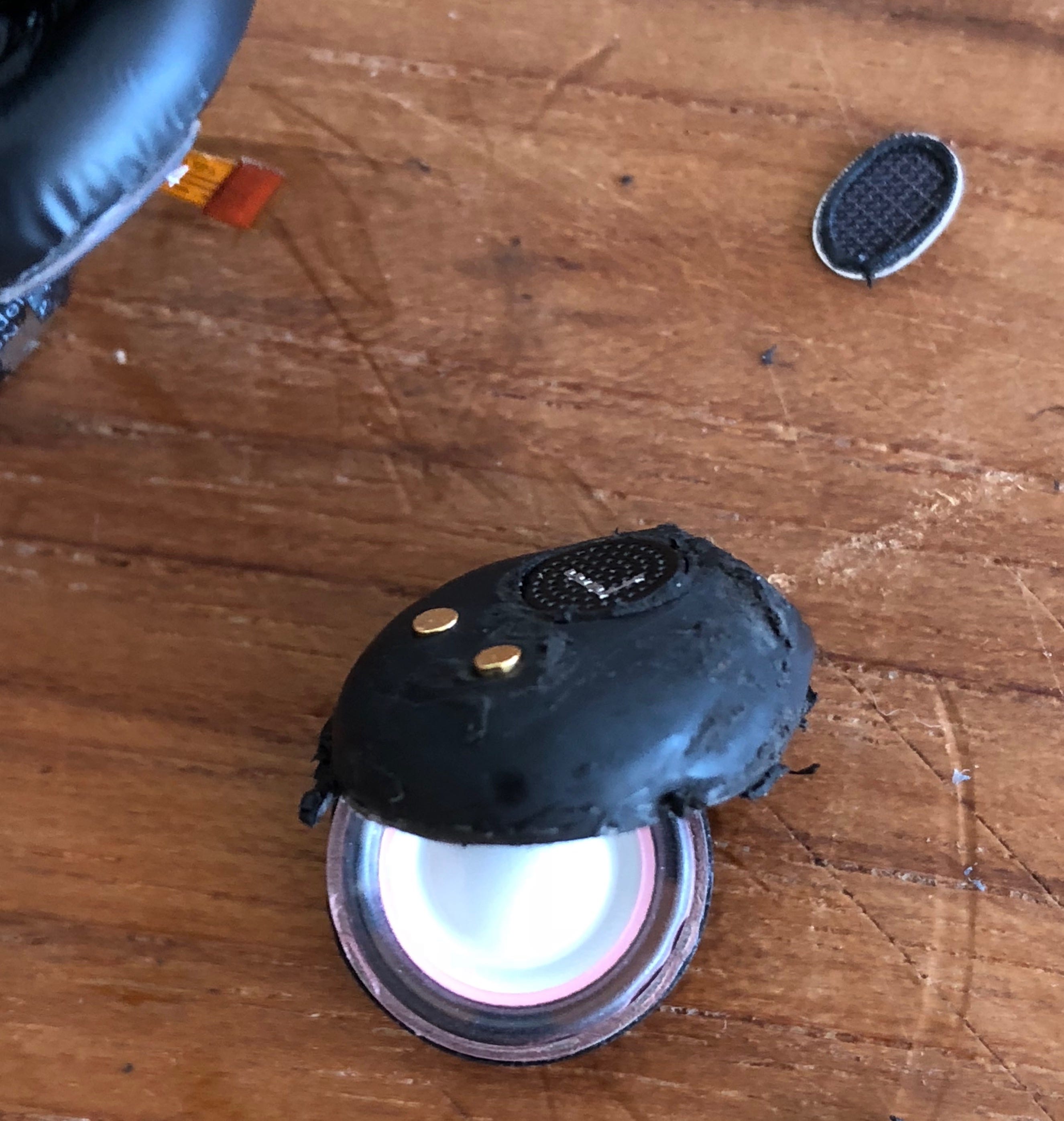
After much heating and scraping, the speaker was revealed rather anticlimactically. Nothing too interesting to see here, other than confirming that the flex cable powered the speaker and connected to the two charging contacts.

The Right Earbud
Lets move to the right earbud and see what we can find. Opening with the similar heating and prying approach, we can see that its already looking a little more interesting…
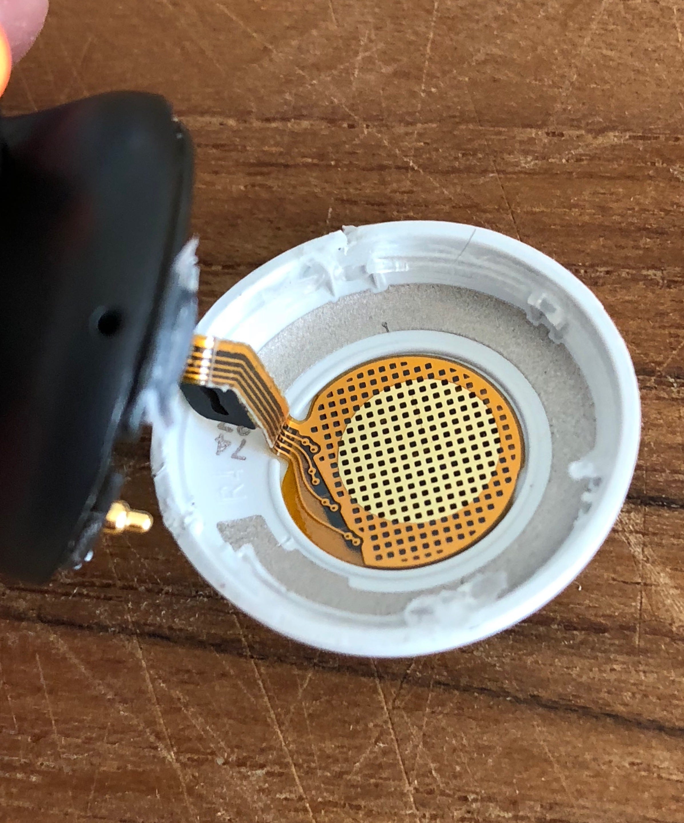
On the interior of the white plastic covering, you can see a silvery metallic ring. This is the antenna, placed in this ideal location to get the best possible signal quality and resultingly Bluetooth range. It is connected to the main PCB by the gold-colored pogo-pin.
But what’s fascinating about the antenna is how it is placed there, using a technique called Laser Direct Structuring (LDS), which allows a conductive antenna to be effectively “printed” directly onto plastic. This is done by adding a small amount of non-conductive metallic compound to the white plastic. A laser is then used to draw out the desired pattern, which causes the metallic compound in the plastic to form a surface that allows other metals to adhere to it by creating nuclei (similiar to how fine particles in the air can cause humidity to be drawn out of the air, seeding rain). By then placing the plastic in a metal bath solution, one can grow precise and even layers of nickel, copper or gold onto the plastic only on the areas that were lasered.
I previously saw this in another teardown of the Doppler Labs Here One:
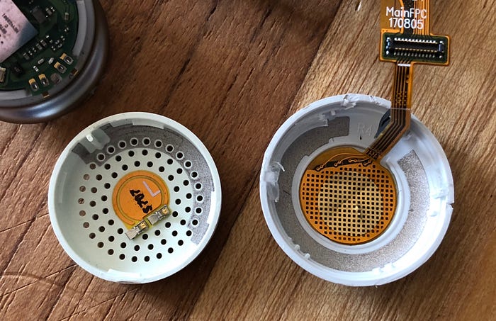
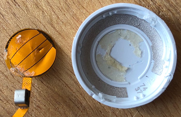
Let’s now take a chance to look at the capacitive touch sensing. One can see that the Here One also has capacitive touch, but has only two contacts, meaning it can only pick up a single tap, whereas the Pixel buds have 5 connections running through the flex PCB strip, so one can assume it can sense a finger’s presence in four different quadrants. (the fifth signal is for ground)
Peeling the flex PCB off its adhesive, you can see that it does indeed have four different quadrants. This is required to accurately detect swiping, i.e. a finger moving across the surface in one direction, for up/down volume control.
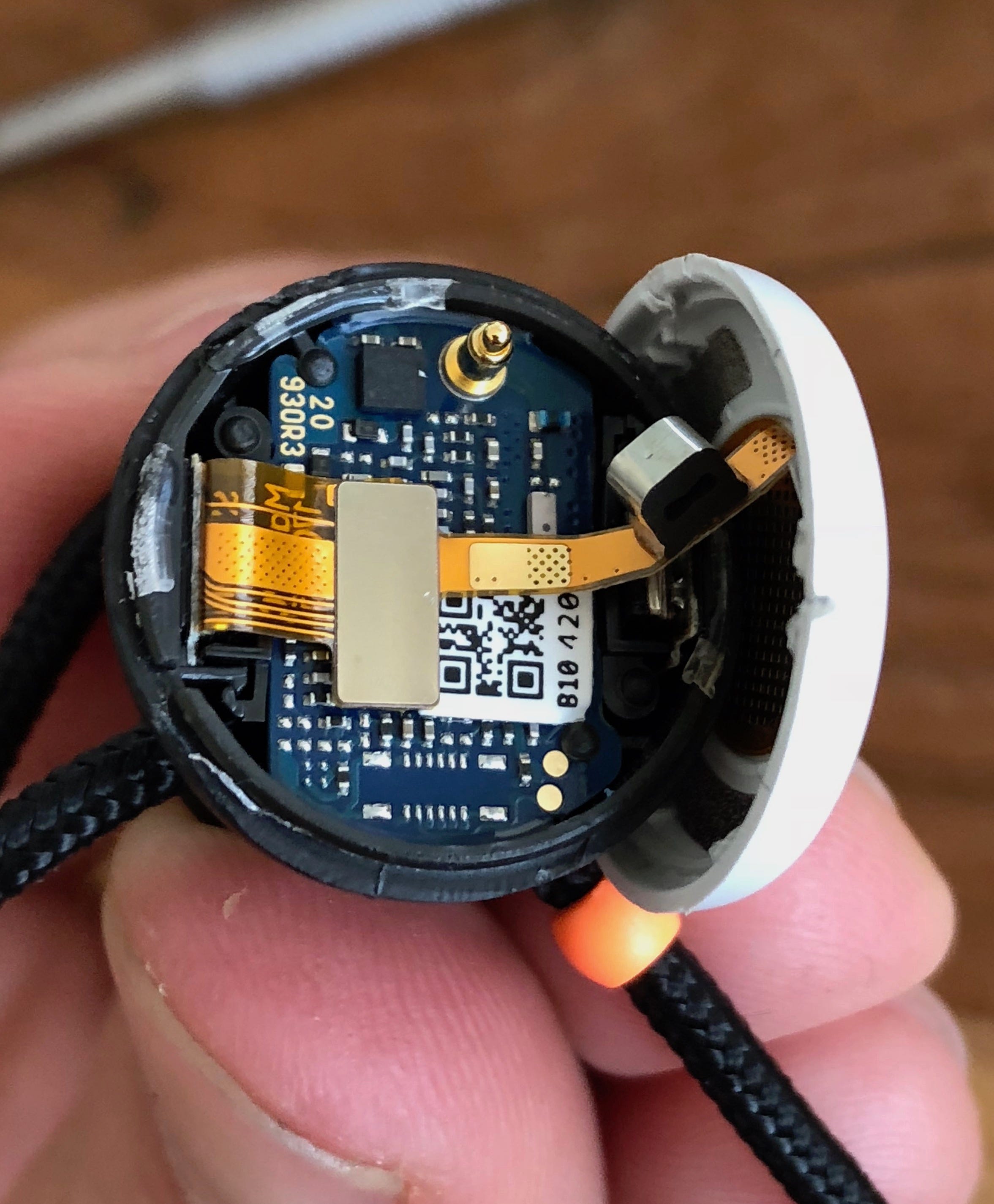
Now returning to the rest of the earbud, let’s reveal the main PCB. This is done by removing a flex header, a QR sticker from the main Bluetooth SoC, and cutting off some little plastic laser-staked rivets to remove the main PCB. This seems to be where the brains of the operation lie — we’ll return to this later…
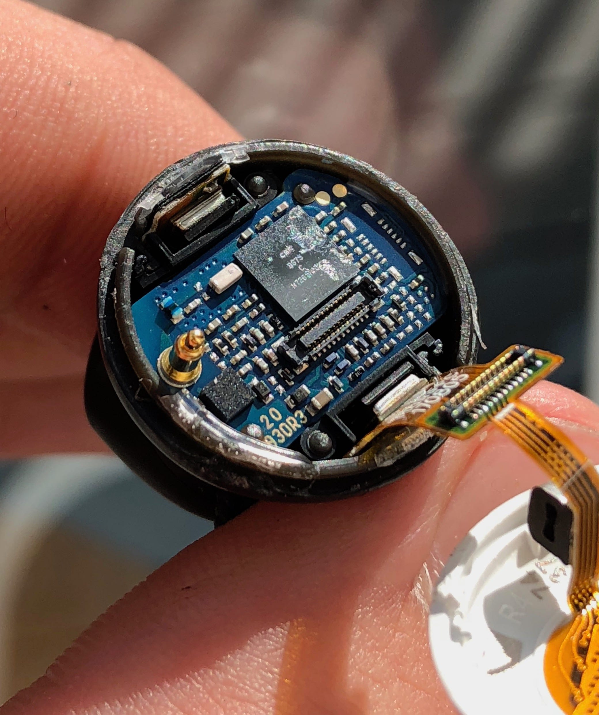

Now we can see a rigid-flex PCB and what appears to be microphones on either side of the earbud. Removing some more plastic fixtures, we can unravel this rigid flex, confirming that these are two bottom-port microphones with some adhesive foam allowing them to create a snug fit against the main body.


This is a really neatly layered design, making use of flex PCB and some clever origami to position microphones and capacitive touch sensing around the main PCB. As in the left earbud, there are flex and wire cables travelling off to the speaker and charging contacts. We’ll leave this intact for now, and take a closer look at that main PCB.
Identifying the chips
Going back to the top of the PCB, we can see the main brains and talk of this product is the all too popular CSR8675, a single-chip solution for audio processing and Bluetooth. We can also see another chip below the gold pogo-pin that is probably significant but only bears what looks like a QR code. We will need to do some “zoom and enhance” detective work later on that one…
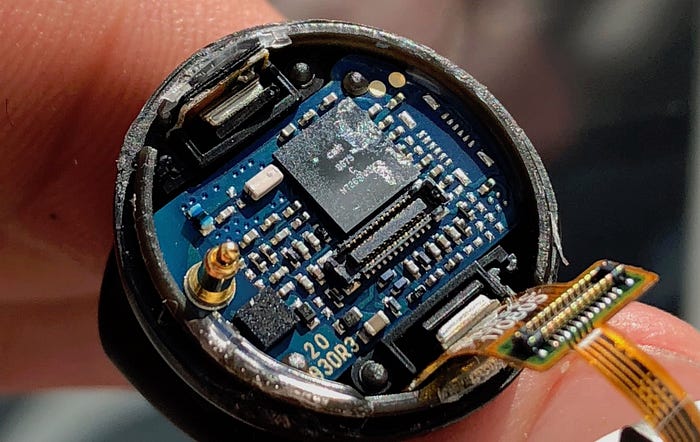
CSR (acquired by Qualcomm a couple of years back), were pretty big in the audio and connectivity space, and I’ve seen this specific chip in other “hearables” such as the Here One, LifeBeam Vi, Nuheara IQBuds, and Bragi Dash to name a few...
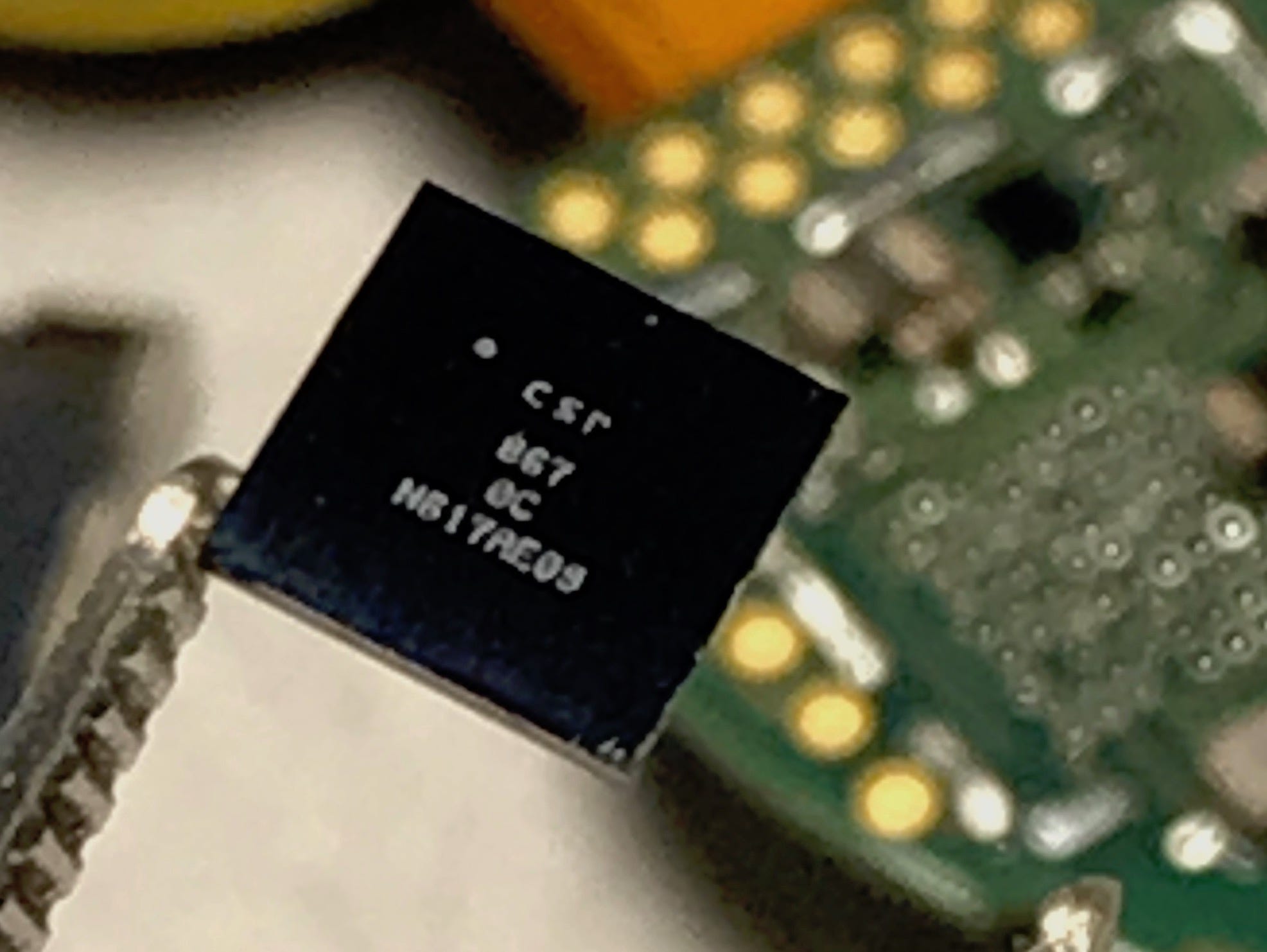
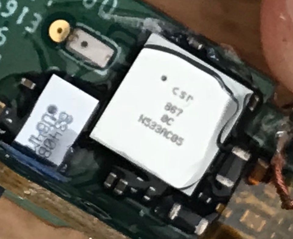
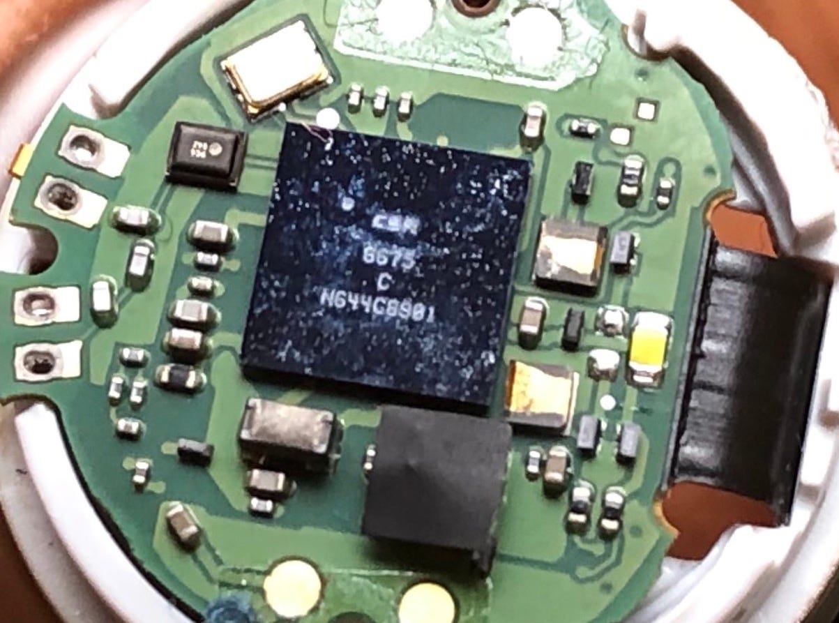
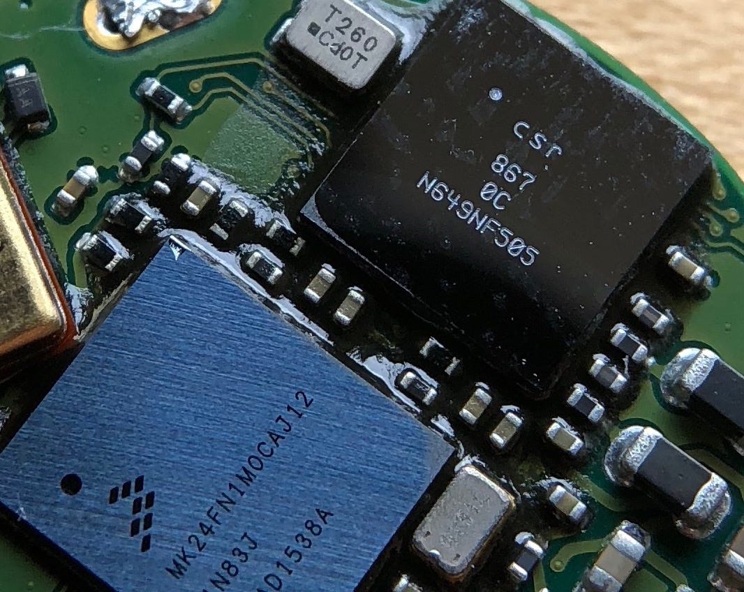
On the reverse side of the PCB, we can see a slew of other chips, namely:

- (CY8C414…) Cypress PSoC 4 S-Series. This most notably contains an ARM Cortex-M0, capacitive touch sensing interfacing, and reconfigurable analog and digital blocks.
- (+8971G …) Maxim Integrated MAX8971EWP+T. This is a compact, and high-efficiency switch-mode charger for the Li-ion cell we saw earlier. The need for high efficiency and flexible input voltage is because the buds are charging from another larger battery in the Pixel Buds case. It’s likely that it is on this board as it interfaces over I2C with the other processors for managing charge parameters, and providing the battery charging status etc.
- (5AC03S …) Texas Instruments BQ27421 Fuel Gauge. This uses an integrated sense resistor and algorithms for determining information such as remaining battery capacity (mAh), state-of-charge (%), and battery voltage (mV). A nice and easy and well-contained approach.
- (TPS734 …) Texas Instruments TPS62743. A high efficiency buck converter, for converting battery voltage to a range required for the IC’s, supporting up to 300mA output, with an ultralow 360nA quiescent (“off”) current
- (3324T…) — RClamp3324T Low Voltage RailClamp and 4-Line ESD protection. This protects the circuitry from any dangerous voltages that could be applied on the charging contacts through static discharge or other means
- 26 MHz crystal — This is used by the CSR8675 to create a clock signal for its high speed DSP operations
- (71940Y U64M )— This part was a mystery, not being able to be easily identified from the marking alone. Let’s try figure out what it is…
What we do know is the flash on the CSR8675 is quite small, and it’s likely that there is a lot of custom code that a software company like Google would want to run, especially to get such good noise cancellation and voice detection from mic’s on only one ear. Therefore they would need some external flash. The “64M” in the marking on this chip is a clue, that this is most likely NOR flash — differing from NAND flash as it allows faster reading, better random access, and is typicall used for code storage. NAND on the other hand (ha!), is mainly used for file storage, and boasts faster writing, and higher density (64MB would be laughable for NAND flash unless you were Marty McFly).
Desoldering the chip, we can get a look at the foot print (i.e. the arrangement of contacts soldered to the PCB). We can see some more agreeable evidence here, as it is fairly common for flash to have 8 pins. (The outer 4 pins are not connected to anything and mostly function as aligning and securing the chip onto the PCB).

If I would make a guess, I would say it is part compatible to the Micron Serial NOR Flash N25Q064. Here is the datasheet exercept showing the footprint of the chip-scale package version of this flash chip. Looks pretty similiar:

We’ll end the detective work there and call this 64M NOR Flash. Now onto mystery chip number 2, with the QR code we saw earlier.
By process of elimination, now that we’ve identified all chips, this would have to be a stereo headphone amplifier, to power the two earbud speakers. But lets see if the QR code reveals some clues. A $10 iPhone microscope lens and Photoshop presents us the following:
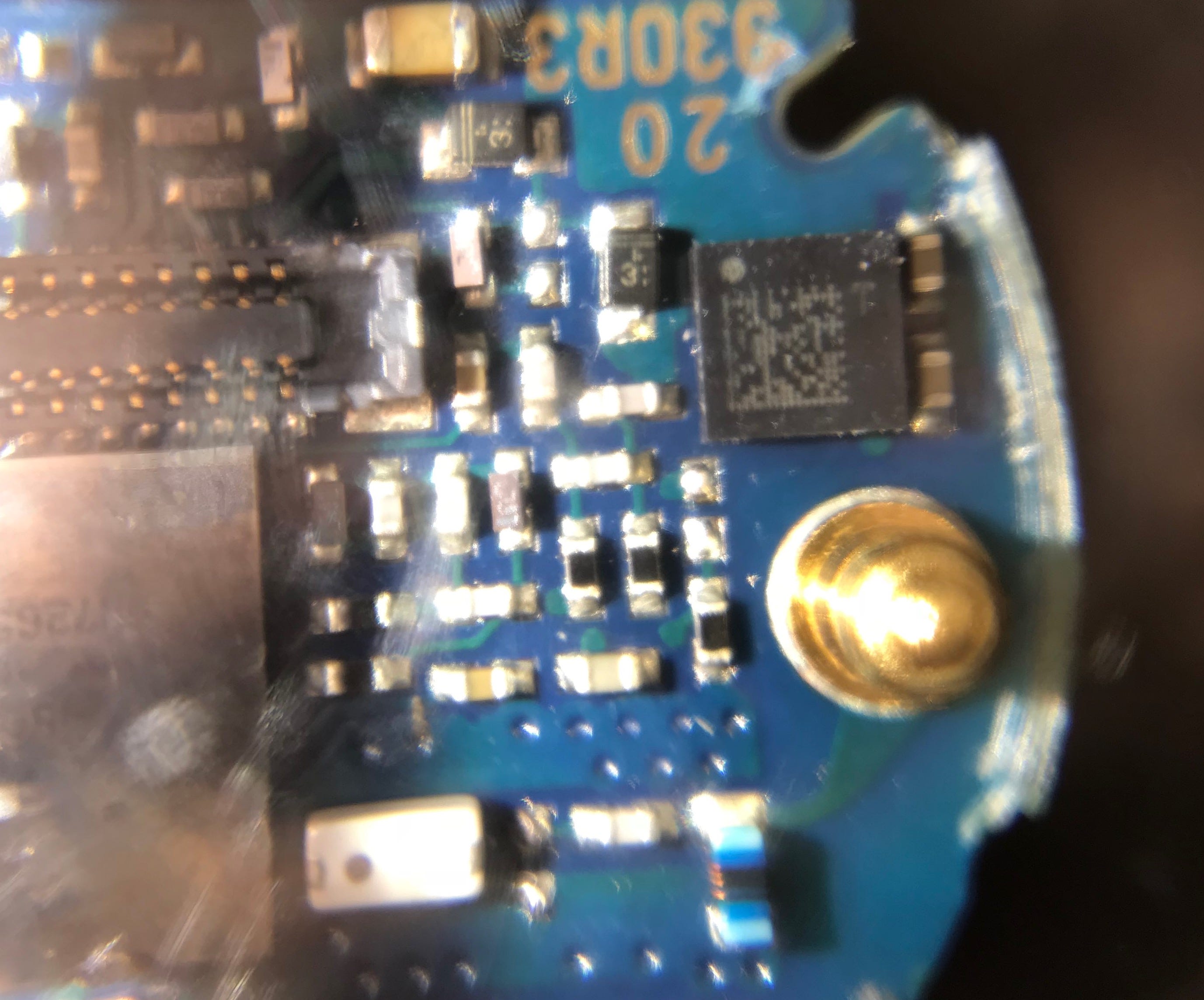

One could do some further cleaning, but this QR code is readable as is, probably sporting a high error correction level, and reads: 787260NW03EA0HE. (Feel free to try it yourself!)
Mean anything to anyone? Not me. Remember, suppliers are not necessarily trying to be difficult, but are not usually incentivized to make teardowns nice and easy. Likely just an ID relating to a batch number.
So let’s desolder the chip and view the footprint:

Doing a parametric search on Digikey/Mouser of 12-pin QFN earphone amplifiers yielded some very similiar looking results of chips that would meet the same requirements, but nothing that looked like an exact match.
Together with the placement of capacitors around the pins, and testing connections to audio lines confirms this is a stereo audio amplifier. Which one, I’m not sure — but there’s not that much to them, and this part was probably chosen due to finding a reliably vetted part and cost optimization of the production line versus innovation-factor.
The microphones
Now let’s take a look at those two microphones we saw earlier. Why two, facing opposite directions? This allows Google to do some better noise cancellation and beam-forming, to focus on only picking up speech from the user. Almost all transmission of audio signals in electronic designs today are digital, to avoid noise — as most modern designs are compact and have wireless radios in close proximity. These microphones have optimally designed sampling built-in, and conversion to a binary means of encoding called pulse-density modulation (PDM). In this scheme there is a clock signal sent to the microphones, meaning that two microphones can share the same data channel, in which one asserts the data line on the rising edge of the master clock, while the second asserts on the falling edge, meaning only one input pin is required on the DSP and these two signals are highly synchronised — necessary for the beam-forming algorithms. Remember how the human ears can locate a sound’s direction by the different time at which the soundwaves reach either ear? Timing is important here…
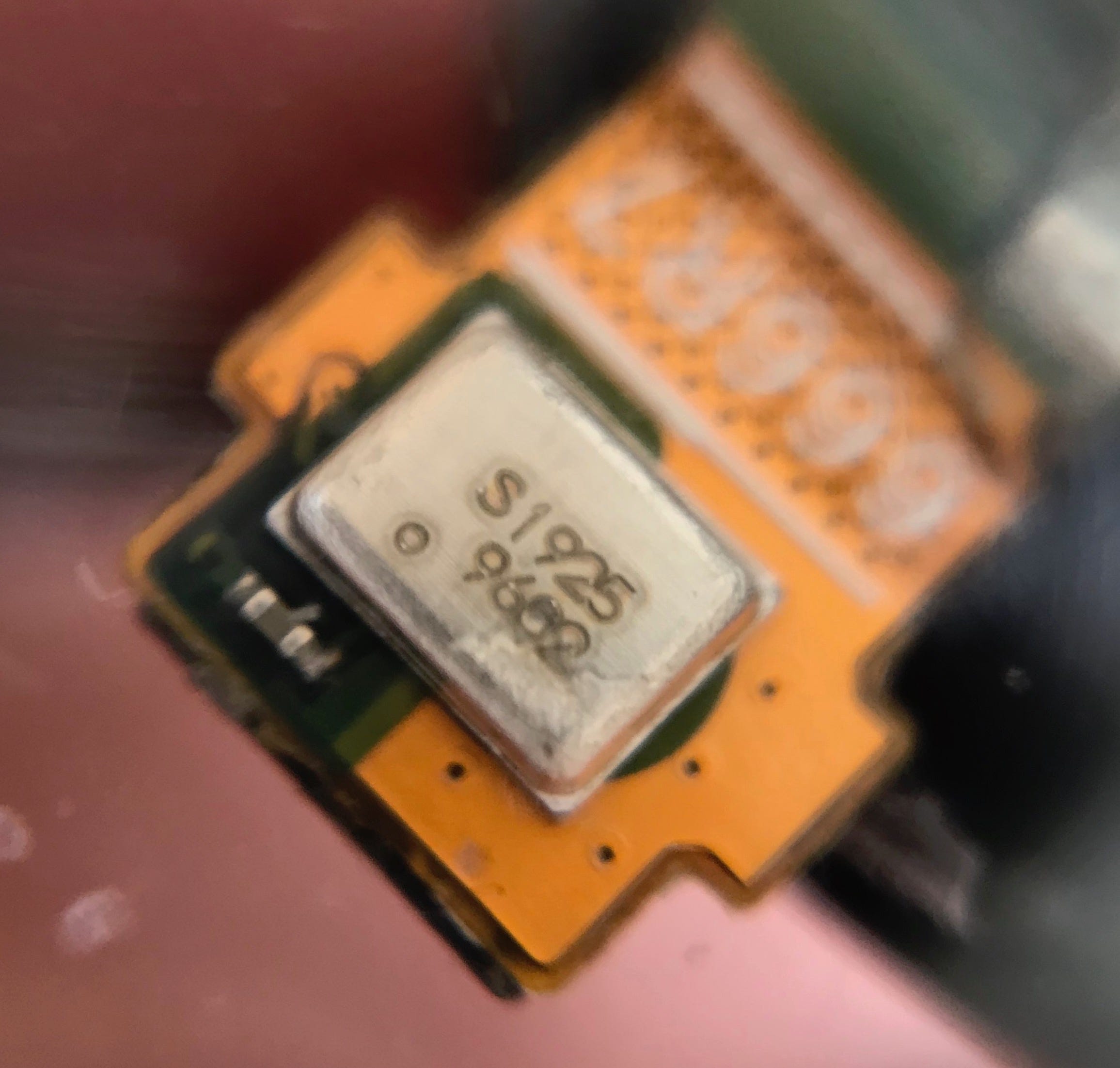

The markings don’t do much to identify the microphone and manufacturer, but I can tell this is from Knowles, and part of their SiSonic range of MEMS mic’s.
In the string S1925 9602, the “S” indicates it is a production ready version from the SiSonic range, whereas the number is just for batch identification. To figure out what type of mic it is, let’s desolder it. Knowing the dimensions, that it is a bottom port digital mic and from the footprint below, we can narrow it down to likely being the SPH0641LM4H-1. (Interesting note, if they used the ultrasonic version, the SPH0641LU4H-1, they might have been able to do some interesting things with using higher than perceptible frequencies to learn about whether the earbud is in the ear or not, assuming the speaker create such frequencies)

Lets go one step deeper down the rabbit hole, and remove the metal shield to see what’s inside this mic…
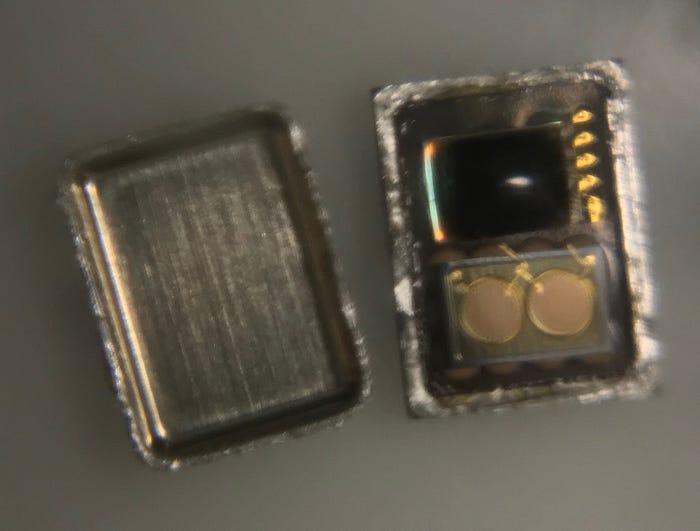
Here we can see the the transducer and the ASIC (circuit customized for a particular use, in this case digitizing the audio signal from the transducer). The faint gold lines are connectors “wire-bonded” to the transducer and ASIC, and essentially the only part of this whole signal chain to carry analog signals to the DSP.
Lets take a moment of silence for the buds and eulogize:
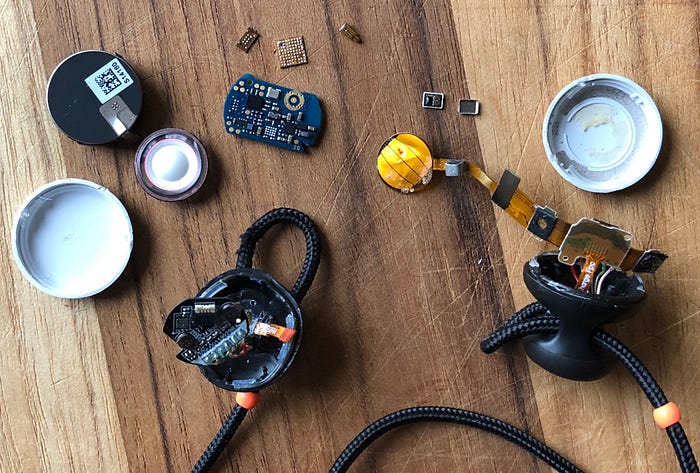
The Pixel Buds were cleverly designed and really interesting to take apart. While they used glue, they used significantly less than the AirPods and so were slightly easier to open up — and this could potentially be done while maintaining repairability, although reducing the waterproofing unless you could recreate the seal.
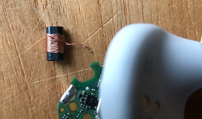
One can also see now how having the connecting string between left and right sides eases the hardware design challenges, such that the battery can be in one ear and the brains in the other. Having one larger battery is more power, space and cost efficient than having one in each. Secondly, there is no need to manage wirelessly syncing between the two buds, again saving power, space and cost. Some products achieve this by having redundant Bluetooth chips, where both will connect to the phone, or only the one with the best signal (depending on which pocket your phone is in) will connect and broadcast to the other. But most use what is called NFMI (Near Field Magnetic Induction), defined as “short range wireless physical layer that communicates by coupling a tight, low-power, non-propagating magnetic field between devices”. This is well suited as the buds stay at a fixed small distance (between your two ears) and the magnetic field is not affected by the large amount of water in your head to the same extent as a Bluetooth signal would be. This however requires a large coil in each earbud, again taking up precious space, and doesn’t include other data, such as if the second earbud needed to have a microphone for improving beamforming and noise cancellation.
Interaction improvements?
After tearing down the Pixel Buds, let’s take a look at some possible interaction improvements or alternatives. How might one add detection of whether they are in your ear? The Apple AirPods use infrared sensors to detect this, which would be the first idea. Some quick ideas:
- Capacitance — can be used to sense the edges of an earbud being pressed against the outer ear canal, and would differentiate well between skin and other surfaces, i.e. as in a bag or on a table. The placement of these capacitive sensors would need some careful mechanical design.
- Humidity differential — with humidity sensors becoming cheaper, and more power efficient (possibly becoming cheaper or at least lower power than IR detection), one could tell if a surface of the product was pressed against skin.
- Accelerometer — the earbuds are in a pretty consistent orientation when inserted — and even if hanging upside down, you can assume they’d be in the same orientation relative to each other. Once they were determined in the ear by one or more of the other methods, the accelerometer could be used to tell if there is unexpected movement with a low-power and fast response, prompting a re-evaluation of whether they are in or not (similiar to how an altimeter in GPS helps prompt a re-evaluation of altitude).
- Ultrasonic — more of a “creative” approach, having two microphones, you could learn a lot about the earbud’s location from measuring the response from small ultrasonic chirps. This would only work for the right ear in the current version.
Furthermore, for gestures, an accelerometer could provide a redundant means for sensing taps, or one could make use of deliberate squeezes of the bud to pause/play/activate assistant, to differentiate from accidental taps.
Lastly, having always-on listening for a wake-word (i.e. “Ok, Google”) so you won’t need to tap may seem power intensive but is becoming more feasible. I’m making a prediction that future versions will have this, based on some of the low-power DSP’s with built-in Deep Neural Net hardware acceleration being developed by chip manufacturers.
With the earbuds now violated beyond repair, let’s finally wrap-up with the case…
The case
No clean way to do this, so with a little bit of hacking and a few cuts, we can pop out the inner plastic from the fabric shell, which is attached using snaps. The fabric shell looks like it is made from a combination of vacuum-forming, injection molding, in-mold textile application, followed by application of a soft-touch finish to give that smooth velvety feel.
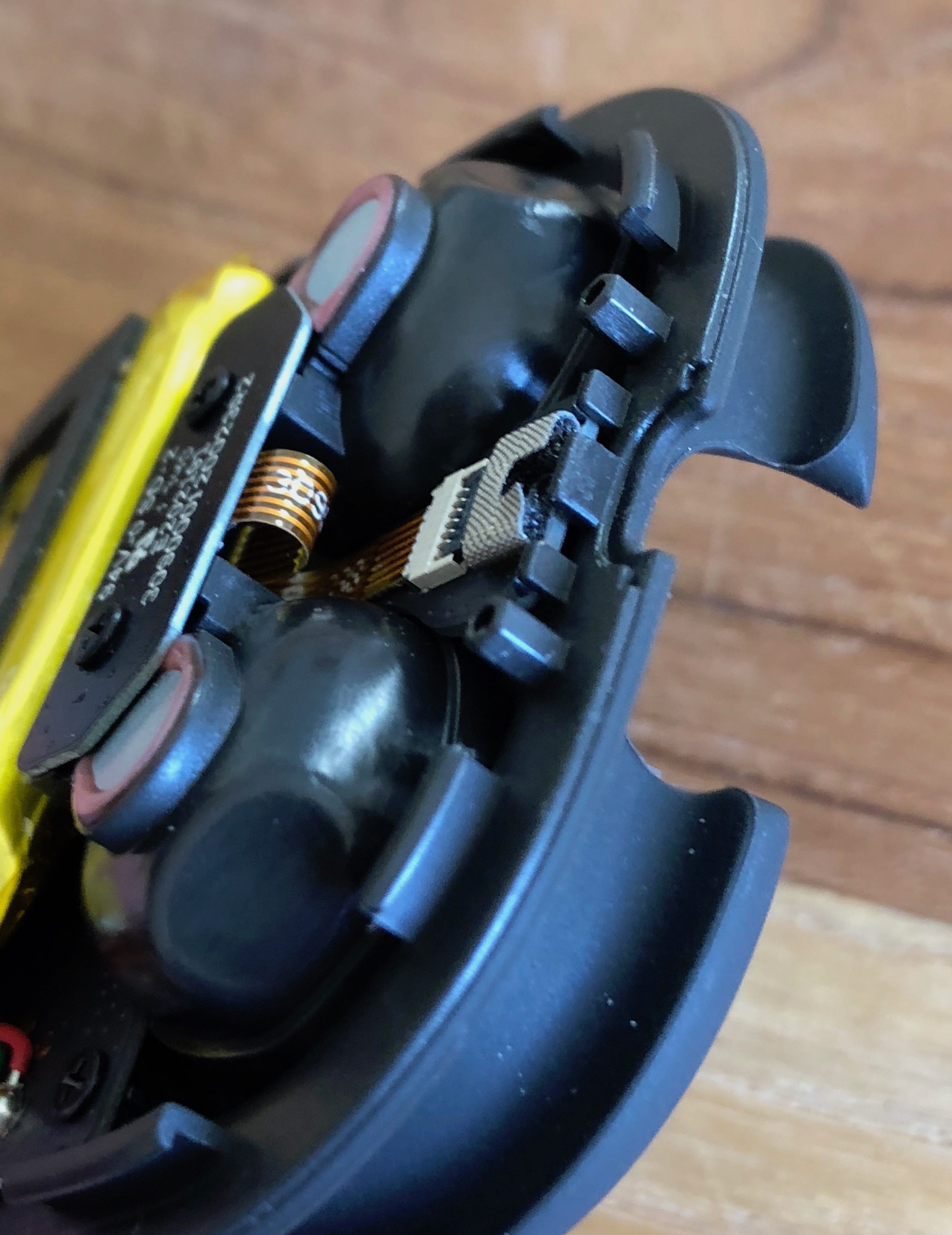
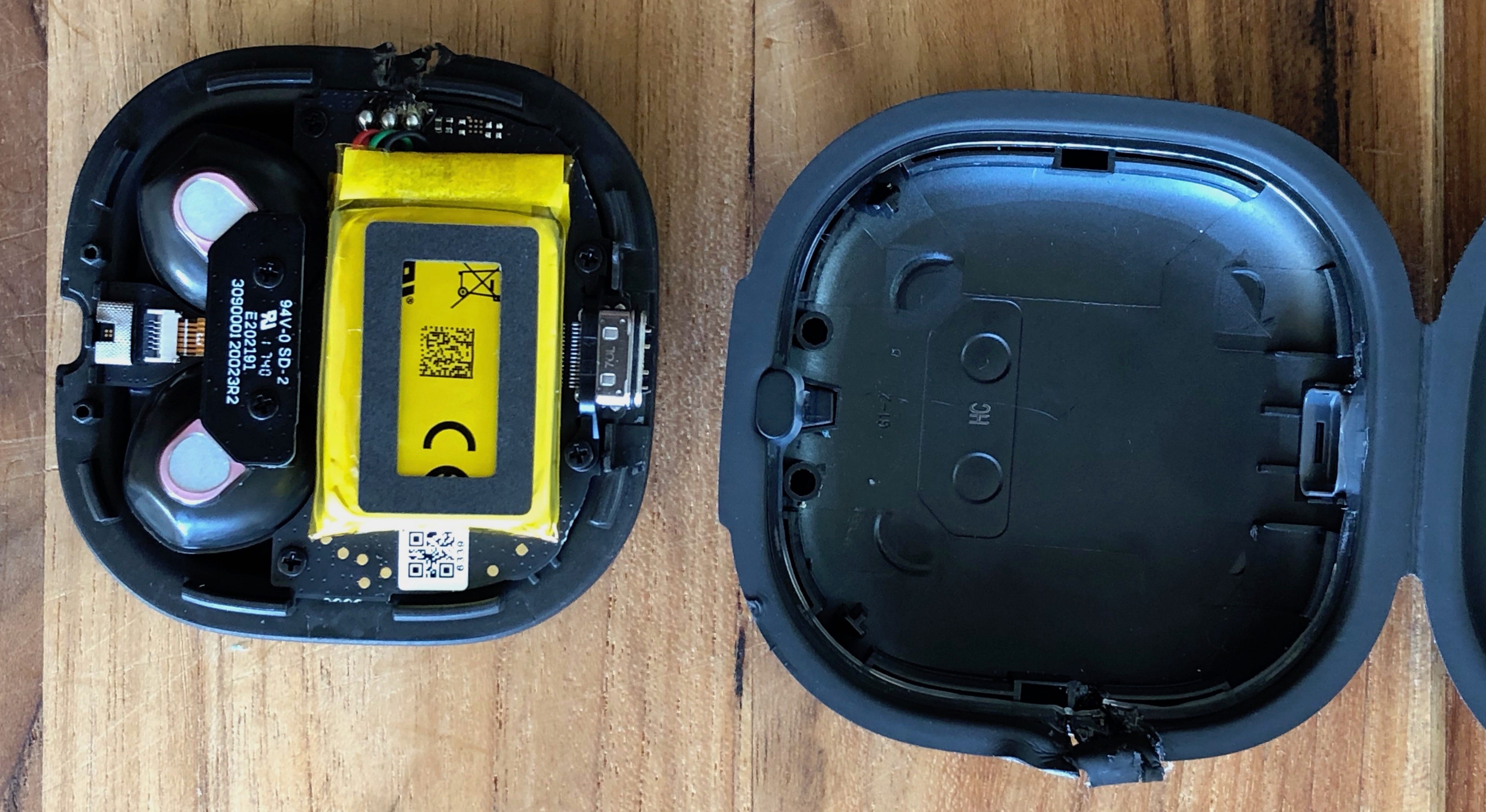
We can see a 2.39Wh Li-ion Polymer battery, the USB-C header, a smaller PCB for mounting the charging contacts, and what must be a small subassembly for magnetically detecting whether the box is open or not. Notice how USB-C has 12 visible pins. There are another 12 pins not seen, (commonly through-hole), for a total of 24, or 12 per insert orientation, (Yes, it finally doesn’t matter which direction you plug in USB-C), compared to 4 pins for previous USB versions.

Unscrewing the main PCB, we can start to identify some more components on the reverse side.
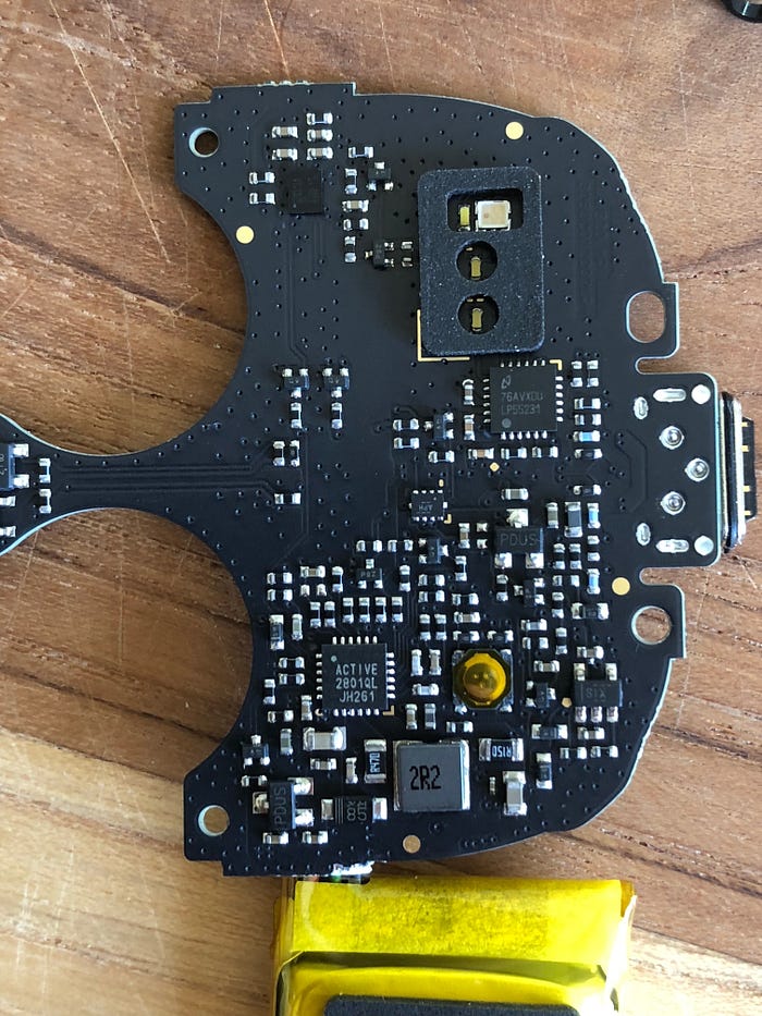
- (CY8C414…) Cypress PSoC 4 S-Series. The same ARM Cortex-M0 containing chip seen in the right earbud. Some features are likely not needed, but they would get a better price, and it would be simpler from a firmware development perspective to double up on this chip, assuming they are using the same factory in Shandong for both the buds and case.
- Active-semi 2801QL 5V/1.5A Backup Battery Pack Manager. This is a nice chip that, according to the datasheet, “integrates all of the functions that a battery pack needs , including switching charger, boost converter and LED indication.”
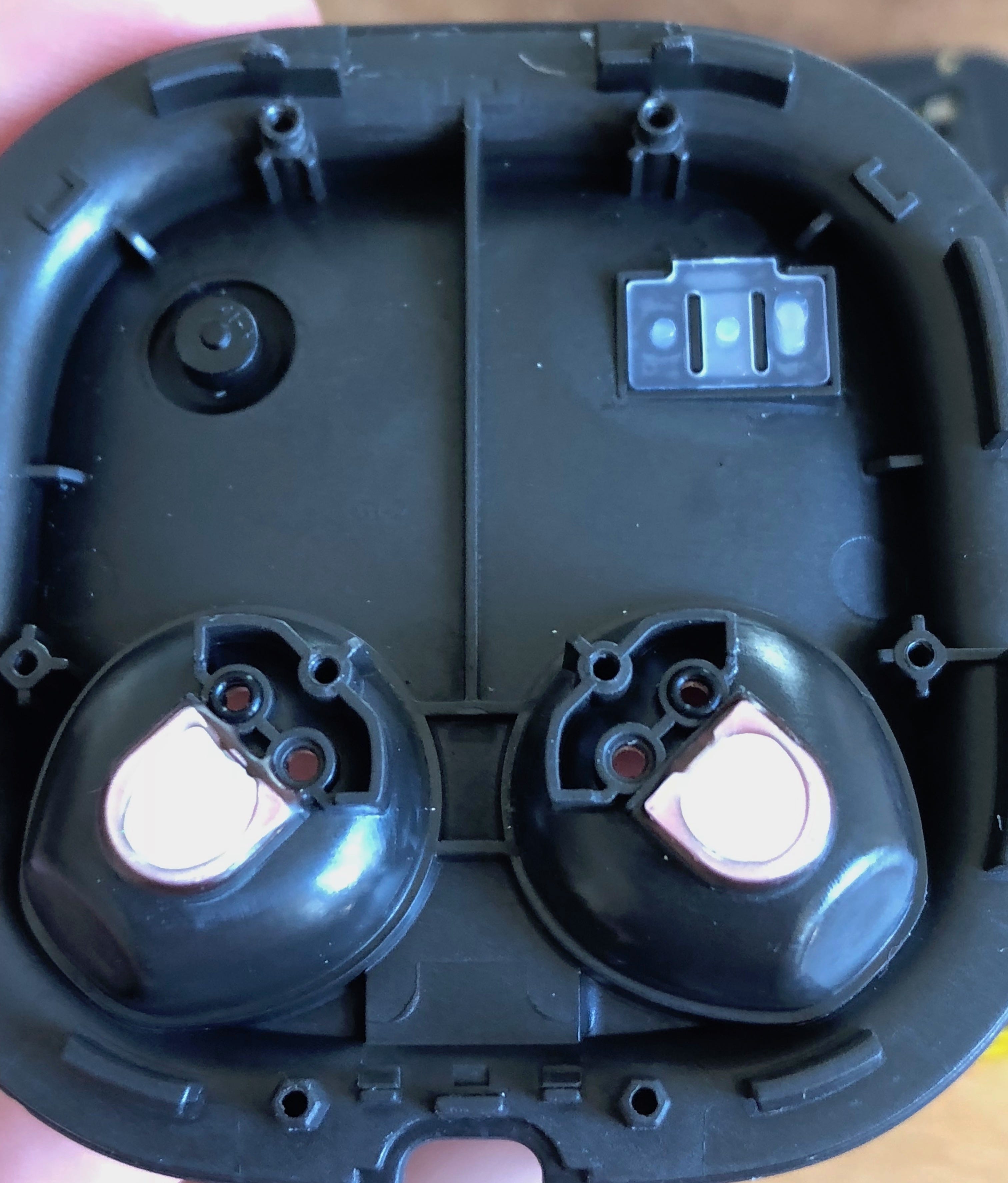
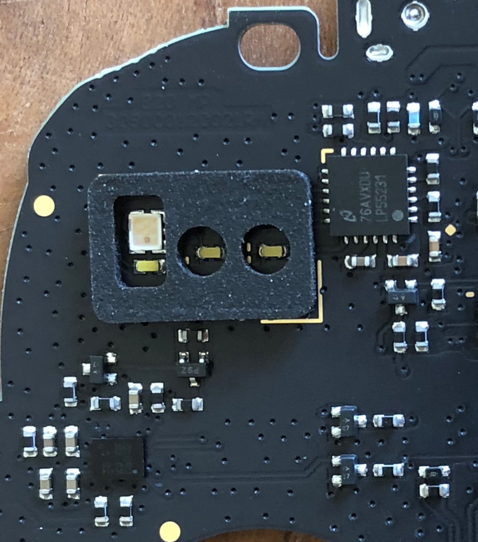
- Texas Instruments LP55231 — 9-channel LED driver. This is used for controlling the 3 white indication LED’s, and an RGB LED, which shares the location of one of the white LED’s. You can see the foam adhesive with three cutouts, which seals the light against the case and light pipes, allowing it to shine through as clean little dots.
- Snap dome button — This is presumably the reset button, you can see that this has a corresponding button built into the plastic case in the picture below.
Conclusion — why a voice interface, or technology you can talk to?
The Google Pixel Buds received some mixed reviews. But for being a voice interface and as an enabler of Google’s AI assistant, they have made some big leaps and deserve that recognition in a pretty tough market.
Big ideas in technology typically need a few stepping stones in-between the present and the end goal. Each stepping stone takes advantage of the “adjacent possible” of current technology, while providing some marketable value to sustain progress for future versions. Some stepping stones falter, and sometimes feet get wet (ahem, Google Glass), but all help drive the industry forward and expand the realm of adjacent possible to allow further innovations.
If one end goal is humans being able to interact with computers — that are becoming more ubiquitous and integrated into everything around us — and do so at a higher bandwidth, we stand a chance to not be left behind and benefit more greatly from some of the amazing benefits and capabilities of AI. Whether this actually ends up being the “neural lace” or not, a worthy stepping stone to get there is earbuds that can understand how we communicate, allowing technology to adapt to humans, and not the other way around.
Again, I hope this teardown was helpful — continuing into the New Year I’m hoping to help make technology more accessible, for both people who are interested in building it, and the people who have the most to gain from it. It’s easy to look at some technology coming out of Silicon Valley, or historically NASA and other institutions for example, and fail to see the bigger picture or application in the rest of the world, but the advances and the possibilities these products open up for innovation in other markets is usually invaluable, as long as we help spread it.
Huge thanks and hat tip to the product designers at Google, and I apologize that this is the second product of yours I’ve publicly taken apart, (3rd if you include Nest?) but as there is a scrapheap of products I haven’t written about, it means there is something about these products worth writing home about… 👏🙇🏻♂️
And to sign off, something that has pleasantly surprised me is how many non-hardware or even non-technical people enjoyed reading these teardowns. So if you liked this article please clap away by clicking on the clapping hands logo as much as you desire, or share this article wherever you can. It helps an obscurely niche article reach more people! And as always feel free to contact me with any comments, suggestions or questions at j@justinalvey.com or @justlv on Twitter.
Other teardowns I’ve done:
Google Home Mini
Nest Thermostat E
